
Industrial manufacturing: Optimization of flexible, foil-based magnetic field sensors
The transfer project converts the technology of modular sensors, developed by project S1, into a manufacturing orientated environment. Hereby previous results from fundamental research are transferred into an industrial
application and their suitability is evaluated. This includes the deployment of a new packaging approach in order to adapt the sensors to new application scenarios.
This project aims to further develop magnetic field sensors with regard to industrial requirements concerning design specifications for the assembly as well as funcionality and stability.
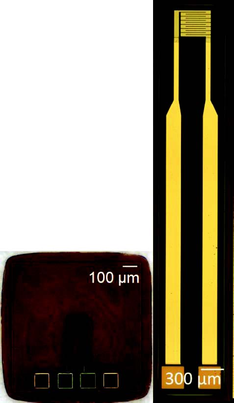
The production process developed in project S1, is being applied in this project as well. The process implies that first a polymer is spin coated on a silicon wafer. On this polymer the sensor is deposited consisting of the meander shaped functional layer, the feed lines and the contact pads. As protection of the sensor and as an isolation layer, another polymer is spin coated on top. To separate the substrate into single sensors, the silicon wafer is being dry etched from the backside, creating a silicon grid, which exposes each microsystem and simultaniously grants a mechanical stability until the separation takes place.
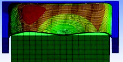
The separation process or rather the therefore necessary machine is being developed and fabricated together with an industrial partner named ETO Magnetic GmbH. The separation is performed by stamping. A planar stamping tool and a planar counter support clamp the microsystem. A simultaneously performed movement of stamping tool and counter support realizes a damage free detachment of each sensor.
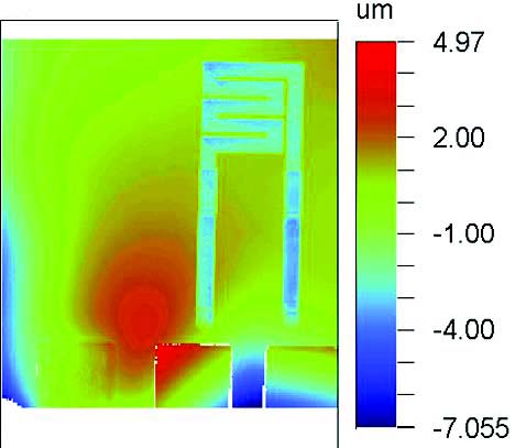
The separated sensor elements are very filigree. Each system has a thickness less than 15 μm with outside dimensions of 5x1 mm2. For handling the separated sensor, a vacuum channel is integrated into the counter support, which is used to transport the sensor to its final application area, where the sensor will be placed and fixed with a suitable adhesive.
These flexible and very thin sensors, produced in the described way offer opportunities for the user to gain measurement data from previously inaccessible areas. For example could these sensors be used to be placed in a narrow air gap or on uneven surfaces. By being able to access these new areas and thus being able to measure more data, additional information about processes can be gained. These information will help to improve future product generations.
Industry partner


78333 Stockach
78333 Stockach


