Optoelectronic integration of radio frequency communication systems
One vision of the industry 4.0 is the idea that the production process of a component adjusts itself flexibly to modified framework conditions and that the manufacturing conditions are constantly improved. This requires the components to be clearly identifiable and locatable. Furthermore, it is beneficial to save production data as well as component loads directly on the component and transmit these data to an external infrastructure through a wireless connection. Therefore, the Institute of Radiofrequency and Microwave Engineering (HFT) investigates new concepts for component-integrated communication systems (Figure 1), which is done in cooperation with the Institute of Transport- and Automation Technology (ITA).
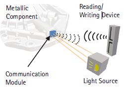
The major objective is to enable a metallic component to save and process component-relevant data and information during the entire lifecycle and exchange those with its surroundings. The data transmission between the component and the reading/writing device is wireless and is achieved to electromagnetic waves. Here, as operating frequency, the worldwide allowed ISM band at 24 GHz is used. The energy supply is ensured through the sole use of a solar cell. In comparison to conventional wireless based systems, this is advantageous as the communication module works without batteries. If the ambient light is sufficient, the system can be operated without external light sources. In order to enable a continuous process monitoring of load parameters such as temperature or strain, it is possible to add additional sensor systems to this module resulting in a self-sufficient wireless sensor node. The task of processing and saving data as well as communicating with the environment is accomplished by an ultralow-power microcontroller.
So far, a bidirectional data transmission with a data rate of 80 kbit/s and a transmission range up to 0.5 meters could be achieved.
In order to expand the range of applications, a new design concept is investigated in the current funding period (Figure 2). The antenna and RF circuit are structured on a glass substrate with the thickness of 200 μm and directly positioned on the solar cell located underneath. Ideally, the antenna and the RF circuit should have a high optical transparency to minimize the effect of shadows on the solar cell. Furthermore, the individual layers are to be connected electrically. This connection technology can be integrated directly into the housing, which is realised by a three dimentional molded interconnect device (3D-MID) simultaneously acting as the carrier of the digital circuit.
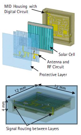
A comparison of both concepts shows that the new design reduces the installation volume significantly (Figure 3). Current research results prove that the communication range and the data rate can still be increased.

Subproject leader