
Direct deposition of ultrathin sensor systems onto components of arbitrary size
Future components should be able to gather data during their manufacturing process as well as during their product life cycle. This enables them to monitor their conditions, to react for instance by calling for inspection and to provide relevant data for optimizing future component generations.
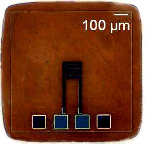
To achieve this, sensors are required that enable the components to detect a variety of measurands. Within the subproject S1, research has been carried out to develop modular, multifunctional micro sensors. In the first research period, amongst others, temperature, strain and magnetic field sensors were developed. The sensors were fabricated on stiff silicon carrier substrates, that were replaced by thin polymer foils as carrier substrates during the second research period (figure 1). This was done to increase the level of system integration and the flexibility. The overall thickness including the adhesive layer was reduced from 500 μm to 15 μm (figure 2).

In the third research period, the focus is set on the deposition and structuring of sensors directly onto the surface of components. Within another project, the flexible, polymer-based magnetic field sensors are adapted and improved with respect to industrial requirements (compare transferproject T05, page 9). Sensors directly deposited onto the surface of components need no carrier substrate and no glue compared to silicon- and polymer-based sensors. Hence, the influence on the measurement results caused by these layers are eliminated. The overall thickness of the sensor depends on the surface roughness and the required insulation layer thickness and is usually not thicker than a few micrometers. Hence, these thin sensor systems allow for instance an application at positions within machines where the available space is limited.
Research is carried out to identify requirements and challenges for a direct deposition and structuring on technical surfaces. To achieve optimal properties of the insulation and functional layers, material- and systemspecific parameters for the deposition process have to be investigated. Especially, the high surface roughness of a few micrometers is challenging. It requires an adequate sealing of the deposition process to the atmosphere and a sufficient electrical insulation layer.
Moreover, the structuring of the sensors by using shadow masks has to be investigated. In particular, the repeatable repositioning and the structural resolution are of interest. An apparatus for depositing and structuring sensors directly onto components of arbitrary size has been invented and constructed (figure 3).


